MOSFET Working | Animation With Java Applet Simulation
MOSFETs (Metal Oxide Semiconductor Field Effect Transistor) are of four different types or modes. They may be enhancement or depletion mode or maybe N channel or P channel. How does a MOSFET work? Here we provide a Java applet tutorial of N channel enhancement mode MOSFETs. This article explains the exact working principle of MOSFET with an interactive animation using java applet technology (MOSFET working animation). MOSFETs are used in your motherboards, for example, to generate CPU Voltage, Memory Voltage, etc. So it is essential for an electronic hobbyist to know the working of a MOSFET. MOSFETs are voltage-controlled power devices whereas bipolar transistors are current-controlled devices. Gate controlling is clearly demonstrated in this java applet example of MOSFET.
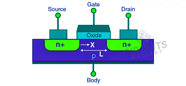
MOSFET Working
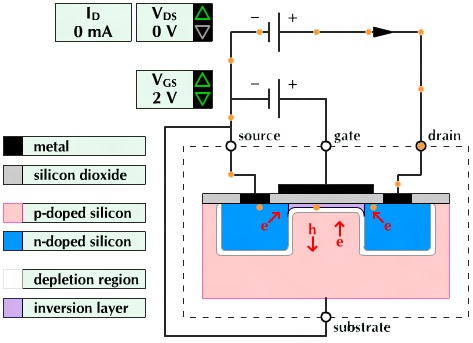
- If no positive voltage is applied between gate and source the MOSFET is always non-conducting.
- The conductivity of the pathway from source to drain is controlled by providing a voltage between the gate and body of the semiconductor.
- The electric field produced by this applied voltage is spread throughout the insulating layer of SiO2 (Silicon Di Oxide).
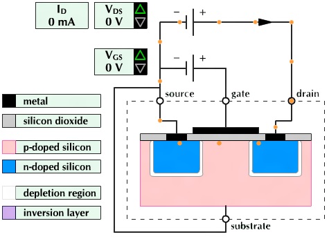
What Happens if we increase VDS while VGS=0V in MOSFET
- Applying VDS with 0 VGS will affect Zero current because the PN junction between N doped drain and P doped substrate is reverse biased.
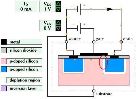
- The only effect of increasing VDS with zero VGS is to enlarge the width of the depletion region close to the drain end.
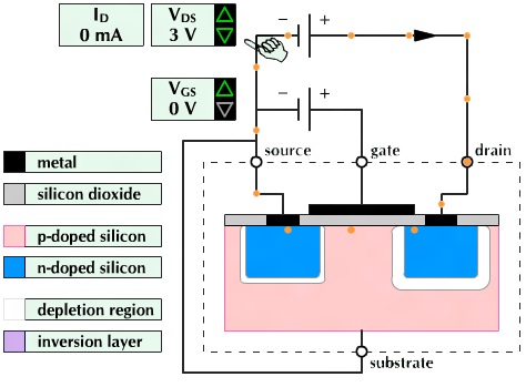
- Even though there is no channel, a small reverse saturation current will flow through the reverse-biased PN junction.
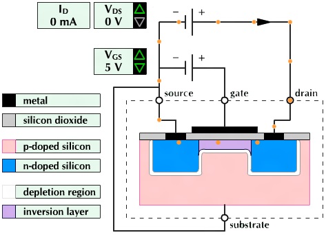
Effect of VGS in the formation of the Inversion layer in MOSFET
- Rising VGS produces an electric field that repels holes from the P doped substrate and attracts mobile electrons from the N doped source and drain regions.
- Thus an N-type conducting channel is formed between the source and drain region once VGS>VT. (VT: – Threshold voltage). This layer is called the Inversion layer.
Increase VDS by keeping VGS constant
- The voltage between the gate and the channel is smaller at the drain end than at the source end when increasing VDS
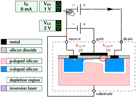
- With VGS=VT, the inversion layer is merely just formed. The channel, therefore, is said to be pinched off due to the reduced field strength at the drain end.
- In this situation, there is no current flow.
Increase VGS keep VDS constant
- A superior VGS boosts the number of mobile electrons inside the channel, increasing the width of the inversion layer.
- Increase VDS: Ohmic region and channel length modulation in MOSFET– For little VDS, the drain current increases linearly with VDS, this is called an ohmic or linear region.

- While increasing VDS the reverse bias effect is greater at the drain end, as a result, the inversion layer is tapering deeper at the source end than at the drain end.
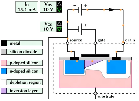
- At the pinch-off point, the inversion layer depth at the drain end is shrinking to zero.

- An additional increase of VDS causes the pinch-off point to shift towards the source, dropping the effective length of the channel. This effect is called channel length modulation.

- Saturation is attained for a large value of VDS. At saturation, MOSFET acts as a current source, with ID free of VDS and controlled by VGS (Hence the name Voltage controlled device).
- Are you feeling bored while reading this article? Don’t worry the Java applet interactive animation of MOSFET will help you to understand these concepts easily.
Conclusion
Here we’ve discussed step by step process of construction and working of MOSFET. Hope you get the idea and implement it in your future projects.
Subscribe to our newsletter
& plug into
the world of circuits
![What Is the Purpose of the Additional 4 Pin Connector on Your New Power Supply [Decoding The Mystery]](https://www.circuitsgallery.com/wp-content/uploads/2023/07/What-Is-the-Purpose-of-the-Additional-4-Pin-Connector.webp)
Excellent way to explain, how MOSFET wok. It will be much easier for my students to understand.
I’m glad to hear that the explanation was helpful for your students! If they have any more questions or need further explanations on MOSFETs or any other topic, please don’t hesitate to ask.