What Is the Current Through the Transistor | PNP and NPN Transistors
A transistor is a semiconductor device that conducts and insulates electric current or voltage. This active component serves both as a switch and an amplifier. The most prominent application of a transistor is its utilization in controling or regulating the flow of electronic impulses.
The base of an NPN transistor limits the amount of current that flows through it while enabling current to flow from the emitter to the collector. PNP transistors, on the other hand, are designed to conduct current from the collector to the emitter.
Current Flow According to the Construction of Transistors
The construction of transistors is illustrated below. The current flows according to the position of the p-type and n-type material in a transistor.
- To make transistors, three layers of semiconductor material are placed together. Doping refers to the process of adding extra electrons to some layers while removing electrons from others (doped with “holes” – the absence of electrons).
- Because electrons have a negative charge, a semiconductor material with extra electrons is referred to as an n-type, whereas one with surplus electrons removed is referred to as a p-type (for positive). To construct transistors, either a n on top of a p on top of a p or p over n over p is employed.
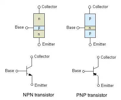
Figure 1: Transistor Construction
- Electrons move from the n-type to the p-type layer through the wire connecting the transistor to the circuit.
Conventional Current Direction in NPN Transistor
The NPN transistor’s objective is to allow electrons to travel from the emitter to the collector (such that conventional current flows from the collector to the emitter).
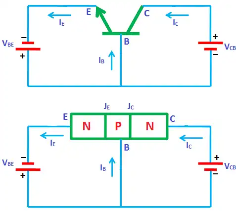
Figure 2: Current flow in an NPN transistor
The base, which controls how many electrons the emitter “emits,” gets electrons from the emitter. The collector “collects” the bulk of the electrons released and transfers them onto the next component in the circuit.
Conventional Current Direction in PNP Transistor
A PNP works in a similar but opposite manner. The base continues to govern current flow, but it now flows from emitter to collector in the opposite direction. Instead of electrons, the emitter produces “holes” (a hypothetical absence of electrons), which are received by the collector.

Figure 3:Current flow in an NPN transistor
Operation Modes of Transistor
Bipolar junction transistors (BJTs) and metal-oxide-semiconductor field-effect transistors (MOSFETs) are the two basic types of transistors that can operate in different modes. The mode of operations depends on the polarity of the DC voltage. The modes of the transistors are described below.
| Transistor | Modes | Direction of Current |
| BJT | Cut-off Mode: Both junctions are reverse-biased in this mode, thus no current flows through the device. As a result, the transistor is in the off state and functions as an open switch. This mode is used to turn off an application. | From the emitter to the collector (NPN).From the collector to the emitter (PNP). |
| Saturation Mode: Both junctions are forward-biased in this state, thus current flows through the device. As a result, the transistor is turned on and operates as a closed switch. This mode is used for turning on the switch. | No current | |
| Cut-off Mode: There is no current flow between the drain and source in this mode because the gate voltage (VGS) is less than the threshold voltage (VTH). | From the emitter to the collector (NPN).From the collector to the emitter (PNP). | |
| MOSFET | Linear Region or Triode Mode: VGS is greater than VTH in this mode, but the drain-to-source voltage (VDS) is smaller than the pinch-off voltage (VP). The current between the drain and source is proportional to VGS in this mode. | No current. |
| Saturation Mode or Active Mode: VGS is bigger than VTH in this mode, while VDS is greater than VP. The current between the drain and source is no longer proportional to VGS in this mode, and the transistor functions as a voltage-controlled resistor. | NMOS: Source to DrainPMOS: Drain to Source | |
| Saturation Mode or Active Mode:VGS is bigger than VTH in this mode, while VDS is greater than VP. The current between the drain and source is no longer proportional to VGS in this mode, and the transistor functions as a voltage-controlled resistor. | NMOS: Source to DrainPMOS: Drain to Source |
Frequently Asked Questions and Answers
How Do I Calculate the Base Current in a BJT Circuit?
When the input voltage to a transistor is around 0.6 V, the BE junction starts to conduct. The collector current is determined by the base current IB, which is limited by the base resistor RB: IC= βIB.
Because the supply voltage connected to the collector through RC is substantially higher than the input voltage, the BJT is in forward active mode, ensuring that the base-to-collector (BC) junction is reverse-biased.
What Is the Difference Between DC and AC Currents in a Transistor Circuit?
AC and DC both describe different forms of current flow in a circuit. The electric charge (current) in direct current (DC) only flows in one direction. Electric charge in alternating current (AC), on the other hand, alternates direction on a regular basis.
The DC current shows the operating point of a transistor. And, as for the AC current, it carries the amplitude to be amplified or to be switched.
How Does the Collector Current Vary With Temperature in a Transistor?
An estimated relationship for the change in collector current is as follows: a rise in temperature causes an increase in the minority carrier current but a decrease in VBE Therefore both effects result in an increase in collector current with temperature.
Conclusion
The base of an NPN transistor controls the amount of current that flows through it while enabling current to flow from the emitter to the collector. In contrast, PNP transistors are designed to allow current to flow from the collector to the emitter.
Subscribe to our newsletter
& plug into
the world of circuits
![What Are The 3 Wires On A Microwave Transformer [Answered]](https://www.circuitsgallery.com/wp-content/uploads/2023/11/What-Are-The-3-Wires-On-A-Microwave-Transformer.webp)